You're all caught up—no notifications available.
Explore All Exams at KGS

All Exams
Explore All Exams at KGS
Khan Sir Courses
Geography I Polity I History | World Map I Indian Map I Economics I Biology
UPSC & State PSC
UPSC I BPSC I UP-PSC I MP-PSC
State Exams
UP I Bihar I MP | Rajasthan
NEET | JEE | CUET
NEET | JEE | CUET
Defence Exams
NDA I CDS I CAPF I AFCAT I SSB I Agniveer
Police Exams
UP SI | Bihar SI | Delhi Police | UP Constable
SSC Exams
CGL I CPO I CHSL I MTS I SSC GD I Delhi Police
Foundation Courses
Physics I Chemistry I Biology I History I Geography I Polity I NCERT I Math I English | Map I Reasoning
Railway Exams
RRB | RPF
Teaching Exams
TET | Teaching | UGC
Banking Exams
SBI | RBI | IBPS
Engineering Exams
Civil | Electrical | Mechanical
UGC NET
UGC NET/JRF
Current Affairs provides you with the best compilation of the Daily Current Affairs taking place across the globe: National, International, Sports, Science and Technology, Banking, Economy, Agreement, Appointments, Ranks, and Report and General Studies

SYLLABUS
GS-3: Awareness in the fields of IT, Space, Computers, robotics, Nano-technology, bio-technology and issues relating to intellectual property rights.
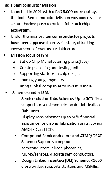
Context: The foundation stone for India’s first advanced 3D chip packaging unit in Bhubaneswar marks a significant milestone under the India Semiconductor Mission (ISM).
About the Advanced 3D Chip Packaging Unit
• First in India: Establishment of the country’s first Glass substrate-based Advanced Semiconductor Packaging Unit in Odisha
• Cutting-edge Technology: Introduction of advanced 3D Heterogeneous Integration modules
• Rapid Progress: Groundbreaking within months of approval by the Union Cabinet, reflecting fast-track implementation
• Strategic Investment: Project outlay of approximately ₹1,943 crore
• Employment Generation: Creation of around 2,500 direct and indirect jobs
• High Capacity: Annual production capacity of 50 million assembled units
• Critical Applications: Chips to serve key sectors including aerospace, defence, artificial intelligence, 5G technologies and Data Centres.
Understanding 3D Glass Semiconductor Technology
• Unlike traditional semiconductor manufacturing, which relies on silicon wafers and planar (2D) packaging, this facility will deploy glass-based substrates and 3D stacking technologies.
• These technologies allow multiple chip components to be vertically integrated, increasing computing power within the same footprint.
• The approach enables heterogeneous integration, where logic, memory, and sensors are combined efficiently. Glass substrates provide better thermal stability, lower signal loss, and higher precision for advanced nodes.
Why This Project is India’s Most Important Chip Bet?
• Technological Shift Beyond Moore’s Law:
• Strategic Importance for India:
Enabling participation in the 3D packaging drive
Supporting critical sectors like AI, 5G, defence, and data infrastructure
Reducing dependence on external technology ecosystems
Future Direction: ISM 2.0
• The government is working on the next iteration of the mission, with a possible outlay of around $11 billion. While ISM 1.0 focused on infrastructure creation, ISM 2.0 is expected to emphasise ancillary industries such as gases, chemicals, and capital goods.
• There is also likely to be a stronger push towards design-linked incentives, with a focus on market-based outcomes and deeper ecosystem integration.
Challenges and Way Forward
• Despite its promise, the project faces several challenges. The semiconductor sector requires high capital investment, advanced technological capabilities, and a skilled workforce.
• India also faces competition from established semiconductor hubs and dependence on global supply chains.
• Addressing these challenges will require sustained policy support, ecosystem development, and long-term investment in research and innovation.
Sources:
PIB
Indian Express
PIB
PIB

The most trusted learning platform on your phone
With our training programs, learning online can be a very exciting experience! Take the next step toward achieving your professional and personal objectives
Course Related Query:
Ask Your DoubtsStore Related Query:store@khanglobalstudies.comNCERT Books
Resources
We love learning. Through our innovative solutions, we encourage ourselves, our teams, and our Students to grow. We welcome and look for diverse perspectives and opinions because they enhance our decisions. We strive to understand the big picture and how we contribute to the company’s objectives. We approach challenges with optimism and harness the power of teamwork to accomplish our goals. These aren’t just pretty words to post on the office wall. This is who we are. It’s how we work. And it’s how we approach every interaction with each other and our Students.
Come with an open mind, hungry to learn, and you’ll experience unmatched personal and professional growth, a world of different backgrounds and perspectives, and the freedom to be you—every day. We strive to build and sustain diverse teams and foster a culture of belonging. Creating an inclusive environment where every students feels welcome, appreciated, and heard gives us something to feel (really) good about.
Get Free academic Counseling & Course Details


